STMicroelectronics Advances Next-Generation Panel-Level Packaging with New Pilot Line in Tours, France
STMicroelectronics, a global leader in the semiconductor industry and a key supplier to customers across diverse electronic applications, has announced a significant step forward in chip packaging and test process technology. The company revealed detailed plans to establish a next-generation Panel-Level Packaging (PLP) pilot line at its Tours site in France. This state-of-the-art facility, expected to become operational in the third quarter of 2026, represents a major milestone in the company’s ongoing strategy to expand manufacturing innovation and secure long-term leadership in advanced packaging.
The Promise of Panel-Level Packaging
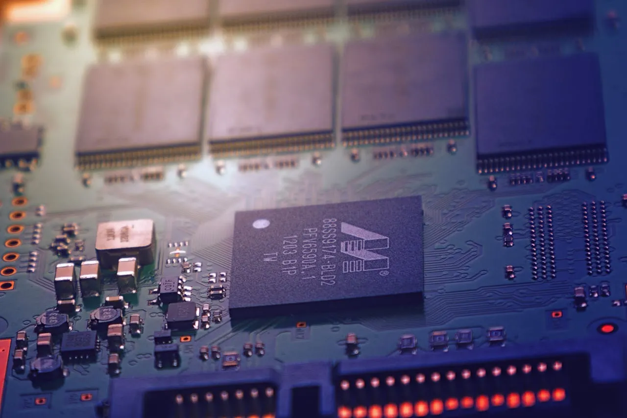
Panel-Level Packaging, or PLP, is a cutting-edge automated chip packaging and test process technology. Unlike traditional wafer-based methods, PLP uses large rectangular panels instead of circular wafers, which allows for higher throughput, improved efficiency, and reduced costs in manufacturing. This breakthrough approach enables the development of smaller, more powerful, and cost-effective electronic devices, making it particularly attractive for industries demanding high-volume, high-performance solutions.
ST has already proven its capabilities with its first-generation PLP line in Malaysia, which has been operating successfully at high volumes. Building on that foundation, the company now aims to take PLP into its next phases of evolution. Leveraging its global technology research and development network, ST intends to extend PLP’s applications to a wider portfolio of products covering automotive, industrial, and consumer markets.
Strategic Expansion in Europe
According to Fabio Gualandris, President of Quality, Manufacturing and Technology at STMicroelectronics, the Tours initiative is a core part of the company’s broader strategy:
“The development of our PLP capabilities in our Tours site is aimed at advancing this innovative approach to chip packaging and test manufacturing technology, boosting efficiency and flexibility so it can be rolled out across a wide portfolio of applications, including RF, analog, power, and microcontrollers. A multidisciplinary team of experts in manufacturing automation, process engineering, data science and analytics, as well as technology and product R&D, will collaborate on this program, which is a key part of a larger strategic initiative focused on heterogeneous integration – a scalable, efficient new approach to chip integration.”
Gualandris also emphasized that ST’s success with advanced chip packaging in Europe is not new. At its fab in Malta, the company has already demonstrated its capability to deliver high-performing packaging and testing technologies. Now, with the new PLP pilot line in Tours, ST intends to further reinforce Europe’s role in advanced semiconductor innovation while reshaping its global manufacturing footprint.
Investment and Ecosystem Collaboration
The development of the Tours PLP pilot line will be supported by an investment exceeding $60 million, which has already been allocated as part of ST’s larger restructuring and manufacturing program. This initiative is not only about expanding capabilities but also about creating synergies with local research and development ecosystems.
Among the most important collaborations is with the CERTEM R&D center, a local innovation hub that will work closely with ST to accelerate PLP development. This fits within ST’s broader strategy of redefining the missions of certain French and Italian sites to ensure their long-term competitiveness and success in a rapidly evolving semiconductor industry.
Why PLP Matters for the Future
The semiconductor industry has long relied on wafer-level packaging (WLP) and flip-chip technologies to connect silicon chips to external circuitry. However, as electronics become increasingly miniaturized and complex, these methods face limits in terms of scalability and cost. PLP addresses these challenges by enabling more chips to be processed simultaneously, significantly reducing costs while improving overall throughput.
STMicroelectronics has been at the forefront of PLP development since 2020, pioneering an advanced version known as PLP-DCI (Panel-Level Packaging with Direct Copper Interconnect). Today, the company’s highly automated production line is capable of handling very large 700x700mm panels, producing more than 5 million units per day at high yields.
Technical Innovation: Direct Copper Interconnect
At the heart of ST’s PLP-DCI is Direct Copper Interconnect (DCI), a process that replaces traditional wire or solder bump connections with direct copper links between chips and the packaging substrate. Copper’s superior conductivity and reliability provide numerous advantages:
- Reduced power losses through lower resistance and inductance.
- Improved thermal management with enhanced heat dissipation.
- Smaller device footprints that enable miniaturization and increased power density.
This technology also facilitates System-in-Package (SiP) integration, where multiple chips can be combined into a single advanced package. As a result, PLP-DCI is not only improving today’s semiconductor performance but also paving the way for entirely new categories of electronic devices.
Strengthening Europe’s Semiconductor Position
By investing in advanced packaging in Tours, STMicroelectronics is also contributing to the strengthening of Europe’s semiconductor ecosystem. With global supply chains under pressure and governments seeking to bolster domestic production, this initiative reinforces Europe’s strategic importance in the semiconductor value chain.
About STMicroelectronics
STMicroelectronics employs around 50,000 people worldwide, including engineers, designers, and manufacturing specialists, working across a fully integrated supply chain. Serving more than 200,000 customers and thousands of partners, the company delivers technologies that enable smarter mobility, efficient energy and power management, and the deployment of cloud-connected autonomous systems.
As part of its long-term vision, ST is committed to sustainability, aiming to achieve carbon neutrality across its direct and indirect emissions (Scopes 1 and 2) as well as in transportation, business travel, and employee commuting (Scope 3 focus). The company also targets 100% renewable electricity sourcing by 2027, underlining its commitment to innovation that also supports a more sustainable future.


