
Rigaku Corporation, a global solutions partner in the field of X-ray analysis systems and a subsidiary of Rigaku Holdings Corporation (Headquarters: Akishima, Tokyo; CEO: Jun Kawakami; “Rigaku”), announced the intensification of its development of metrology technologies for next-generation semiconductors, based on global research environments.
As part of these efforts, Rigaku is collaborating with imec , a leading semiconductor research and innovation hub located in Belgium, under a three-year development program. This initiative will enable Rigaku to refine its cutting-edge radiography technologies, including 3D device metrology, high-sensitivity detection of ultrathin films and trace elements, and non-destructive testing of microscopic defects.
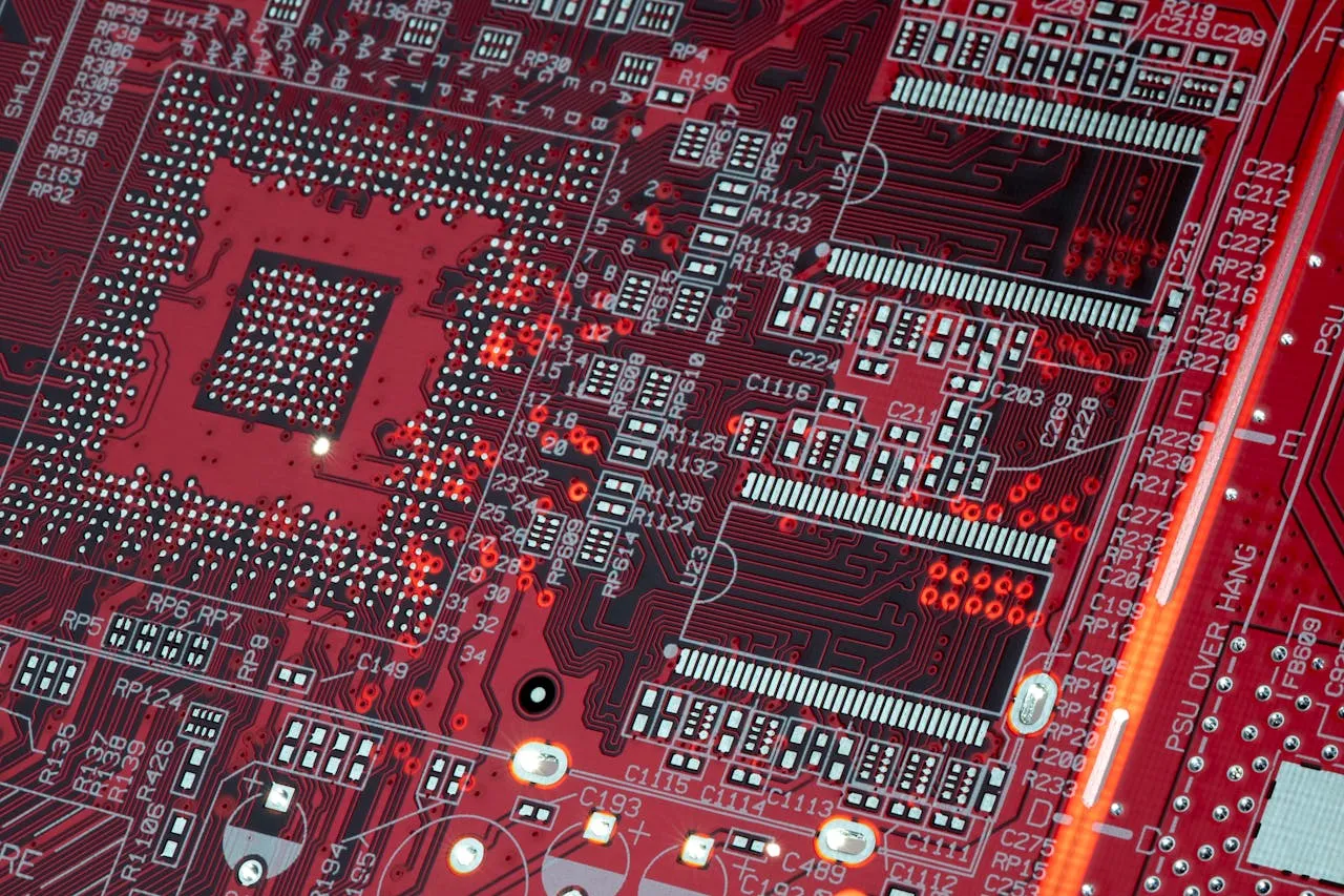
As semiconductors evolve toward advanced architectures such as gate-wrapped (GW) and complementary field-effect transistors (CFETs)<sup> 1 </sup>, and as memory density continues to increase, manufacturing processes become more complex. This evolution generates a growing demand for high-precision, non-destructive measurement and inspection technologies, essential for stable mass production. Rigaku addresses these needs by offering differentiated, high-value-added metrology and inspection solutions.
Key priority areas
- Advanced logic: metrology and inspection technologies for CFET devices
- Metrology of reticles: evaluation of the degradation of photomasks used in EUV 2 lithography
- Advanced cabling and packaging 3 : Non-destructive inspection technologies
- Advanced memory: evaluation of nanostructures in 3D DRAM (a next-generation memory device)
Markus Kuhn, member of the management team and general manager of Rigaku’s Semiconductor Metrology division, stated: “The potential market for Rigaku’s metrology and inspection products for advanced AI semiconductors is expected to reach approximately $1 billion by 2030. To support this growth, Rigaku will continue to launch differentiated, high-value-added products, aiming to capture 50% of this market. Strengthening our collaboration with imec will solidify our competitiveness in high-value-added measurement and inspection solutions and support our medium- and long-term growth.”
1 GAA/CFET: Gate-wrapped field-effect transistors and complementary field-effect transistors. A next-generation device architecture in which n-type and p-type transistors are stacked vertically to increase device density beyond nanosheet (GAA) technology.
2 EUV Exposure: A core technology for advanced semiconductor fabrication that enables the formation of ultrathin circuit patterns.
3 Advanced Packaging: Packaging technologies that integrate multiple semiconductor chips to improve performance and reduce power consumption.
About the Rigaku group
Since its founding in 1951, the engineers of the Rigaku Group have been dedicated to bringing benefits to society through cutting-edge technologies, particularly in its core areas of thermal and X-ray analysis. Operating in 136 countries and regions and employing approximately 2,000 people at nine locations worldwide, Rigaku is a preferred partner for industries and research and analytical institutions. Our international sales account for approximately 70% of our revenue, while we maintain an exceptionally strong market share in Japan. We continue to develop and grow alongside our customers. As applications expand from semiconductors, electronic materials, batteries, the environment, resources, energy, and life sciences to other high-tech fields, Rigaku delivers innovations “to improve our world by opening new perspectives.”
For more details, visit rigaku-holdings.com/english
The text of this press release, being a translation, should not be considered official in any way. The only authoritative version of the press release is the original version in its source language. The translation should always be compared to the source text, which will prevail in case of any discrepancy
Source link:https://www.businesswire.com/