PCB Depaneling Innovation Accelerates with Laser Photonics’ Advanced R&D
Laser Photonics Corporation (LPC), a prominent global developer of industrial laser systems, has joined forces with its subsidiary, Control Micro Systems (CMS Laser), to significantly expand their Printed Circuit Board (PCB) depaneling technology development project. The move aims to address the growing demand for advanced PCB depaneling solutions in the rapidly evolving electronics market.
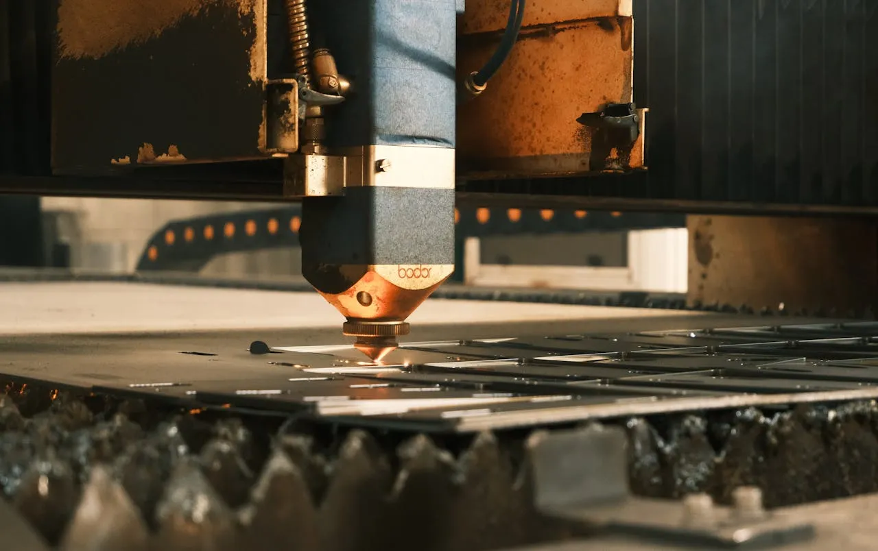
Laser processing has emerged as a highly effective and versatile method for depaneling, offering a multitude of benefits, including precision, narrow kerf width, and non-contact nature. This technology provides a cleaner and more efficient alternative to traditional mechanical methods while eliminating common issues like part-induced stress and the reliance on consumables such as cutting oils. This approach ensures high-quality results, making it an attractive option for PCB manufacturers and electronics assembly lines.
The Advancements in Laser Processing for PCB Depaneling
Laser technology has gained widespread acceptance in the industry for its ability to provide precise cuts without causing mechanical stress to the material being processed. Unlike conventional depaneling methods, which often involve the use of mechanical blades or routers, laser depaneling operates in a non-contact manner. This greatly reduces the risk of damaging delicate components, ensuring that the final product meets the stringent requirements of modern electronics applications.
CMS Laser, with its expertise in laser technology, has developed a custom-tailored depaneling system that offers high speed, pinpoint accuracy, and machine vision alignment. These advanced systems are designed to integrate both CO2 and UV laser types, providing manufacturers with flexibility based on their specific production requirements. The selection of laser type is often determined by two primary factors: the desired cycle time and the cleanliness of the cut edge.
CO2 lasers are typically chosen when speed and cost efficiency are the top priorities. These lasers are capable of making fast cuts, enabling manufacturers to achieve high throughput in short periods. CO2 lasers are especially useful in high-volume environments where cycle time is a critical factor. On the other hand, UV lasers are favored when the quality of the cut edge is paramount. These lasers produce cleaner cuts with minimal charring, making them ideal for applications where high-quality, defect-free edges are required.
As John Armstrong, Executive Vice President of Laser Photonics, stated, “By bringing together the talented engineers and technicians of Control Micro Systems and Laser Photonics, we plan to boost the development of PCB depaneling systems to meet the growing demand in the market.” This collaboration between the two companies is focused on advancing PCB depaneling technology, ensuring that it can meet the evolving needs of manufacturers and offer solutions that enhance production efficiency while maintaining high-quality standards.
The Rise of Laser Routing for Flexible and Sensitive PCBs
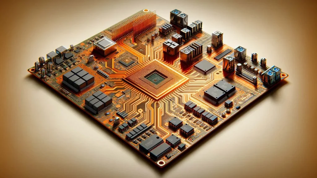
In recent years, laser routing has emerged as a highly preferred method for depaneling flexible and sensitive PCBs used in a wide array of electronic devices. The global shift toward smaller, more compact devices has led to an increased demand for flexible PCBs that can be integrated into miniature electronics, wearables, medical devices, and other cutting-edge products. These types of PCBs require highly precise processing to avoid damage to delicate components such as microchips, connectors, and traces.
CMS Laser’s laser depaneling solutions are particularly well-suited for this application, as they provide the precision and efficiency necessary for processing flexible and sensitive PCBs. The systems are designed to handle intricate designs and smaller form factors, which are common in modern electronic devices. By offering a non-contact solution, laser depaneling minimizes the risk of introducing mechanical stress to the components, ensuring that the PCB maintains its integrity throughout the process.
Furthermore, CMS Laser’s solutions are flexible enough to be used both as standalone machines or integrated into existing Surface Mount Technology (SMT) production lines. This adaptability makes CMS Laser’s systems an attractive option for a wide range of manufacturers, whether they are looking to enhance their existing operations or implement a completely new depaneling solution.
Key Features and Benefits of CMS Laser’s PCB Depaneling Systems
CMS Laser’s Class I PCB depaneling systems are designed with several advanced features that make them stand out in the marketplace. One of the key features is the Through the Optics Vision (TTOV), which provides precise processing and data verification. The TTOV system ensures that the laser beam is accurately aligned with the PCB, allowing for highly consistent results even during high-speed operations. This system enables operators to monitor the entire process in real-time, ensuring that the final product meets all quality standards.
Another significant feature is the CMS Process Engine software, which provides an intuitive, user-friendly interface for operators. The software allows for easy configuration and control of the laser system, ensuring that the process runs smoothly and efficiently. In addition, the software offers optional production line communication capabilities, making it easier to integrate the laser system into larger production environments. This feature helps manufacturers streamline their operations and improve overall efficiency.
Quick setup and easy changeovers are also key benefits of CMS Laser’s systems. The machines are designed to minimize downtime, allowing manufacturers to quickly adapt to changing production requirements. The ability to rapidly reconfigure the system for different PCB designs or materials contributes to high throughput and maximizes productivity. In addition to improving cycle time, the systems offer exceptional accuracy and repeatability, which are critical factors in ensuring high yield and consistent results across production runs.
Expanding R&D Efforts to Drive Innovation
Leveraging CMS Laser’s specialized expertise, Laser Photonics is committing significant resources to research and development (R&D) efforts in the PCB manufacturing sector. This initiative is part of the company’s broader strategy to diversify its offerings and capitalize on emerging market trends. By investing in R&D, LPC aims to further refine and enhance its PCB depaneling technology, ensuring that it remains at the forefront of innovation in the laser processing industry.
LPC’s diversification strategy is designed to address the changing demands of the global market and to enhance its resilience in the face of evolving industry trends. The growing demand for more sophisticated, high-performance electronics has placed an increased emphasis on the need for advanced PCB processing technologies. By focusing on the development of laser-based solutions, LPC is positioning itself as a leader in this rapidly growing segment.
Additionally, the company’s focus on R&D in PCB depaneling aligns with its long-term goals of enhancing shareholder value and building a sustainable business model. By developing cutting-edge technologies that meet the needs of modern electronics manufacturers, LPC is strengthening its position in a competitive market. The company’s ongoing investment in innovation ensures that it remains well-equipped to address the challenges and opportunities that lie ahead in the electronics manufacturing sector.
Looking to the Future of PCB Depaneling Technology
As the electronics industry continues to evolve, the demand for high-performance PCBs is expected to grow at an accelerated pace. Laser-based depaneling solutions, with their precision, efficiency, and flexibility, are well-positioned to meet this demand. With the expansion of its PCB depaneling technology development efforts, Laser Photonics is playing a critical role in shaping the future of PCB manufacturing.
For more information about Laser Photonics’ latest advancements in PCB depaneling technology and other industrial laser systems, visit their website at www.laserphotonics.com.
