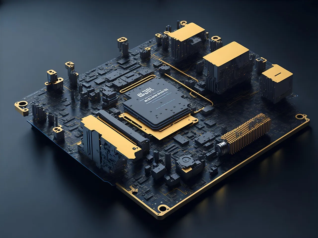
Kioxia Advances Memory Innovation With Breakthrough Technology for Practical High-Density, Low-Power 3D DRAM
Kioxia Corporation, a global leader in advanced memory solutions, has announced a major technological breakthrough that could reshape the future of dynamic random-access memory (DRAM). The company has successfully developed a new class of highly stackable oxide-semiconductor channel transistors, a core innovation that enables the practical realization of high-density, low-power three-dimensional (3D) DRAM. This advancement represents a significant step toward overcoming long-standing physical and economic barriers that have limited the scalability of conventional DRAM technologies.
The new technology was officially presented at the IEEE International Electron Devices Meeting (IEDM), one of the world’s most prestigious semiconductor research conferences, held in San Francisco on December 10. By demonstrating the feasibility of stacking memory transistors in multiple vertical layers while maintaining ultra-low power consumption, Kioxia has laid critical groundwork for next-generation memory architectures designed to support data-intensive applications such as artificial intelligence (AI), cloud computing, high-performance servers, and Internet of Things (IoT) devices.
Rising Memory Demands in the AI Era
The rapid expansion of AI-driven workloads has placed unprecedented demands on memory performance, capacity, and energy efficiency. Modern AI systems process enormous volumes of data in real time, requiring DRAM that can deliver both high bandwidth and massive storage density while keeping power consumption under control. At the same time, edge devices and IoT components demand compact memory solutions that minimize energy use without sacrificing reliability.
However, traditional DRAM scaling approaches are nearing their physical limits. As memory cell dimensions shrink, challenges such as leakage current, refresh power, and rising manufacturing complexity become increasingly difficult to manage. Simply reducing feature sizes is no longer sufficient to meet the growing appetite for memory capacity and performance.
To address these challenges, the semiconductor industry has increasingly turned its attention toward 3D integration—stacking memory cells vertically rather than expanding laterally. While 3D stacking offers a promising path forward, implementing it in DRAM has proven far more complex than in NAND flash memory, largely due to transistor design constraints and power efficiency concerns.
Limitations of Conventional DRAM Architectures
Conventional DRAM relies on transistors that use single-crystal silicon as the channel material. While this approach has enabled decades of memory scaling, it introduces significant limitations when applied to 3D structures. Producing high-quality single-crystal silicon layers in stacked configurations is both technically challenging and costly. As the number of memory layers increases, manufacturing complexity rises sharply, making large-scale production economically unattractive.
Moreover, as DRAM capacity grows, so does the power required to refresh memory cells. DRAM must periodically refresh stored data to prevent information loss, and the energy consumed during these refresh cycles scales with total memory capacity. This creates a fundamental conflict between increasing memory density and maintaining acceptable power efficiency—especially problematic for AI data centers, where energy consumption is already a critical concern.
Recognizing these constraints, Kioxia has focused its research on alternative materials and device structures that can support high-density stacking while dramatically reducing power consumption.
OCTRAM: A Foundation for 3D DRAM
At the previous year’s IEDM, Kioxia introduced Oxide-Semiconductor Channel Transistor DRAM (OCTRAM), a novel memory concept that replaces conventional silicon channels with oxide-semiconductor materials. OCTRAM employs vertical transistors made from oxide-semiconductors, offering improved electrical characteristics and new opportunities for 3D integration.
Building on that foundation, Kioxia’s latest announcement represents a major evolution of OCTRAM technology. In its most recent presentation, the company unveiled a method for creating highly stackable oxide-semiconductor channel transistors that can be arranged in multiple layers, enabling true 3D stacking of DRAM cells. Importantly, Kioxia has already verified the successful operation of transistors stacked in eight vertical layers—a critical proof of concept that demonstrates both feasibility and scalability.
Innovative Materials and Manufacturing Processes
At the heart of this breakthrough is a novel manufacturing approach that leverages mature semiconductor materials while introducing oxide-semiconductors in a highly controlled manner. The process begins with the stacking of well-established silicon-oxide and silicon-nitride films, materials widely used in existing semiconductor fabrication and known for their reliability and manufacturability.
In a key innovation, the silicon-nitride region is selectively replaced with an oxide-semiconductor material—specifically indium gallium zinc oxide (InGaZnO). This replacement process enables the simultaneous formation of vertical layers of horizontally stacked transistors, creating a compact and scalable 3D memory structure.
By relying on mature deposition and processing techniques, Kioxia’s approach addresses one of the biggest hurdles in 3D DRAM development: cost. The ability to reuse proven materials and processes significantly reduces manufacturing complexity, making large-scale production more economically viable than approaches that require entirely new fabrication technologies.
Scalable 3D Memory Cell Architecture
In addition to the transistor technology itself, Kioxia has introduced a new 3D memory cell structure designed to support fine vertical pitch scaling. Vertical pitch—the distance between stacked layers—is a critical parameter in determining overall memory density. By enabling tighter vertical spacing without compromising performance or reliability, Kioxia’s architecture allows for continued scaling of memory capacity within a compact footprint.
This structural innovation is especially important for future memory products, where maximizing capacity per unit area will be essential to meet the needs of data centers and advanced computing platforms. Together with the new transistor design, the memory cell structure forms a comprehensive solution to the challenges of 3D DRAM integration.
Ultra-Low Power Operation Through Oxide-Semiconductors
One of the most compelling advantages of oxide-semiconductor materials lies in their electrical characteristics—particularly their extremely low off-current. Off-current refers to the leakage current that flows when a transistor is in the “off” state, and it plays a major role in determining refresh power consumption in DRAM.
Kioxia reports that the oxide-semiconductor transistors developed for this technology exhibit ultra-low off-current levels of less than 1 attoampere (1aA, or 10⁻¹⁸ amperes). This represents an extraordinary reduction in leakage current compared to conventional silicon-based transistors.
At the same time, the company has demonstrated high on-current performance, exceeding 30 microamperes (μA), ensuring that the transistors can deliver the necessary speed and responsiveness for high-performance memory operations. Achieving this combination of high on-current and ultra-low off-current is a critical milestone, as it enables both performance and energy efficiency to coexist in a single device architecture.
By reducing leakage and refresh requirements, this technology has the potential to significantly lower total DRAM power consumption—an essential benefit for AI servers, hyperscale data centers, and battery-powered edge devices.
Demonstrated Multi-Layer Functionality
Beyond simulations and material characterization, Kioxia has taken the crucial step of fabricating and testing an actual multi-layer structure. The company successfully produced an eight-layer stack of horizontal oxide-semiconductor transistors and confirmed that all transistors within the stack operate as intended.
This experimental validation provides strong evidence that the technology can scale beyond laboratory concepts and move toward real-world implementation. Demonstrating reliable operation across multiple layers is a key requirement for transitioning 3D DRAM from research to commercial development.
Implications for the Future of Memory
Kioxia’s advancement comes at a pivotal moment for the semiconductor industry. As AI workloads continue to grow and energy efficiency becomes a defining metric for system design, memory technologies that can deliver higher density with lower power consumption will play a central role in shaping future computing platforms.
Practical 3D DRAM could enable larger memory capacities within smaller physical footprints, reduce energy costs for data centers, and support the expanding ecosystem of AI accelerators and edge computing devices. By addressing both cost and power challenges, Kioxia’s oxide-semiconductor-based approach positions the company at the forefront of next-generation memory innovation.
Ongoing Research and Development
Kioxia emphasized that this achievement represents an important milestone rather than a final destination. The company plans to continue refining the technology, expanding stacking capabilities, and advancing manufacturing readiness to support eventual commercialization.
Through sustained research and development, Kioxia aims to bring 3D DRAM from experimental validation to practical deployment, unlocking new possibilities for memory-intensive applications across industries.
As memory demands continue to escalate, innovations such as this underscore the critical role of materials science, device engineering, and manufacturing ingenuity in shaping the future of computing.
Source link: https://www.businesswire.com/


