
Gigaphoton Successfully Installs Excimer Laser System for Advanced Semiconductor Packaging at Japanese R&D Facility
Gigaphoton Inc., headquartered in Oyama, Tochigi and led by President and CEO Tatsuo Enami, has announced a significant milestone in the company’s ongoing efforts to support next-generation semiconductor manufacturing. The company revealed that it has successfully delivered and completed the installation of its advanced excimer laser system, designed specifically for semiconductor packaging applications, at a Japanese company dedicated to the research and development of cutting-edge semiconductor technologies. The installation, finalized in November, represents a major step forward in expanding the use of high-precision laser processing tools for advanced packaging, an area gaining increased importance in the global semiconductor ecosystem.
This achievement highlights Gigaphoton’s ability to adapt and extend its core expertise in lithography lightsources to new, rapidly growing segments within the semiconductor industry. For decades, the company has been recognized as one of the industry’s major suppliers of high-performance lightsources for leading-edge semiconductor lithography. By leveraging this foundation, Gigaphoton has developed a dedicated excimer laser optimized for ultra-fine ablation processes—critical operations that enable high-density, high-performance packaging solutions for next-generation chips.
Bringing Lithography Expertise to Advanced Packaging
As semiconductor devices become increasingly complex and heterogeneous, the importance of advanced packaging continues to rise. Traditional 2D chip designs are reaching physical and performance limits, pushing manufacturers to adopt 2.5D and 3D architectures that allow multiple chiplets to be integrated into a single package. These designs require extremely precise micro-processing capabilities, especially when forming micro-vias and trenches on package substrates.
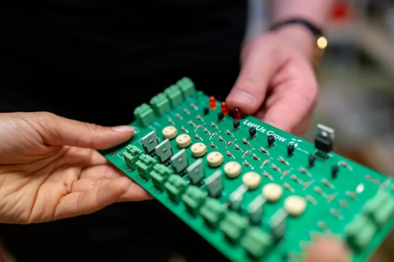
Gigaphoton’s newly deployed excimer laser system, the G300K, is engineered to meet these demanding requirements. Built on KrF excimer laser technology, the G300K operates at a 248 nm wavelength—an optimal range for high-precision laser ablation. The system provides a combination of high power output, fast repetition rates, superior beam stability, and the long operational lifetime required in semiconductor manufacturing environments where uptime and consistency are essential.
By integrating advanced pulse control and energy delivery mechanisms, the G300K enables manufacturers to achieve ultra-fine features such as micro-via holes with diameters of 10 micrometers or smaller, along with highly accurate trench patterns. Such features are indispensable in today’s high-density interposers and substrate technologies that support chiplets and AI-oriented processors. With global demand for AI computation continuing to surge, the need for high-bandwidth, thermally efficient, and compact packaging solutions is growing at an unprecedented pace. The G300K is positioned squarely within this trend, supporting manufacturers seeking to implement new packaging architectures efficiently and reliably.
Integration With ORC Manufacturing’s Processing Equipment
One of the most noteworthy aspects of this deployment is the collaboration between Gigaphoton and ORC MANUFACTURING CO., LTD., a well-established Japanese manufacturer of advanced processing equipment. The G300K excimer laser has been incorporated directly into ORC’s specialized equipment for semiconductor package substrate fabrication, forming a tightly aligned system capable of delivering the ultra-fine, repeatable processing required in advanced packaging lines.
This integration ensures that the laser’s output characteristics—precision, energy uniformity, and long-term reliability—are seamlessly matched with the mechanical, optical, and control systems within ORC’s processing platform. Together, the combined solution offers a turnkey approach for manufacturers seeking to scale their advanced packaging capabilities. The joint presence of both companies in this project highlights a broader industry trend in Japan: the strengthening of domestic capabilities for advanced semiconductor production as the country prioritizes technological sovereignty and competitiveness.
Preparation for Public Demonstration at SEMICON Japan 2025
Gigaphoton announced that the processing results, sample outputs, and detailed performance metrics of the G300K integrated system will be showcased at the exhibition held alongside SEMICON Japan 2025, scheduled to begin on December 17, 2025. SEMICON Japan is one of the country’s largest and most influential events for the semiconductor and microelectronics manufacturing supply chain. The ability to present real processing results will provide customers, partners, and industry stakeholders with a firsthand understanding of how the G300K performs in real-world advanced packaging applications.
This upcoming demonstration is expected to attract considerable interest. As the industry transitions toward increased adoption of advanced packaging for AI, high-performance computing (HPC), automotive electronics, and data center modernization, precision laser processing tools like the G300K are increasingly seen as essential. The SEMICON Japan showcase will therefore serve as a strategic opportunity for Gigaphoton to highlight the system’s value proposition and strengthen its position within the advanced packaging market.
Gigaphoton’s Vision for Expanding Excimer Laser Applications
Commenting on the successful installation and the company’s broader strategy, President and CEO Tatsuo Enami emphasized Gigaphoton’s commitment to continuous innovation. He noted that while the company has long been a core supplier of lithography lightsources, it has also been actively exploring new fields where excimer laser technologies can play a transformative role.
According to Enami, Gigaphoton’s research and development activities are not confined to lithography alone. Instead, the company is broadening its technological scope, investigating various industrial and scientific applications where high-power excimer lasers can deliver unique advantages—particularly in microfabrication, materials processing, and ultra-precise ablation.
He reiterated that Gigaphoton aims to accelerate its efforts to expand into emerging markets and contribute meaningfully to the semiconductor industry’s evolution. As chip design becomes more diverse and manufacturing complexity increases, the need for advanced, reliable, high-precision lightsources will only grow. Gigaphoton intends to remain at the forefront of this transformation by continuously developing next-generation excimer laser systems and enabling new manufacturing processes.
Enami stated, “As a critical lightsource manufacturer in the semiconductor manufacturing industry, we will continue to contribute to the industry through continuous research and development on new processes to facilitate the further implementation of excimer lasers.” His remarks underscore the company’s long-term vision: to play a central role in the adoption of advanced laser processing technologies across the entire semiconductor value chain.
Strengthening Japan’s Position in the Global Semiconductor Sector
The installation of the G300K at a domestic R&D facility is also strategically significant from a national perspective. Japan has been actively investing in revitalizing its semiconductor manufacturing ecosystem, with major initiatives focused on advanced foundries, packaging technologies, and key supply chain components. Companies like Gigaphoton, which supply essential photonics technologies used in chipmaking, play an important enabling role in this broader strategy.
By transferring cutting-edge laser technology to a Japanese semiconductor research organization, Gigaphoton is helping strengthen the technological capabilities necessary for domestic innovation. This supports Japan’s goals of building a more resilient, competitive semiconductor infrastructure and reducing reliance on overseas technologies.
Source link: https://www.businesswire.com/