
DNP Joins Rapidus Funding Round to Accelerate Japan’s 2nm Semiconductor Ambitions
Dai Nippon Printing has announced its participation as an investor in the latest funding round of Rapidus Corporation, reinforcing Japan’s national push to establish advanced domestic semiconductor manufacturing capabilities. The strategic investment is designed to support Rapidus as it transitions from its current research and development phase toward full-scale mass production of cutting-edge 2-nanometer (2nm) logic semiconductors by 2027.
This move represents a significant milestone in strengthening Japan’s semiconductor supply chain resilience while also deepening collaboration between two major industrial players committed to next-generation chip innovation. By entering the funding round, DNP not only provides financial backing but also signals its long-term commitment to contributing advanced materials and process technologies that are essential for realizing high-performance semiconductor manufacturing at the most advanced nodes.
Strategic Alignment Around 2nm Mass Production by 2027
Rapidus has set an ambitious roadmap to achieve mass production of 2nm-generation logic semiconductors within the next few years, positioning itself as a key player in the global race toward ultra-fine process technologies. DNP’s participation in the funding round aligns directly with this roadmap, ensuring that critical upstream components—particularly extreme ultraviolet (EUV) lithography photomasks—are developed and supplied with the required precision, reliability, and scalability.
As semiconductor geometries continue to shrink, the technical complexity of mask fabrication increases dramatically, demanding advanced materials science, nanofabrication accuracy, and defect control capabilities. DNP’s expertise in precision processing and materials engineering will play a pivotal role in enabling Rapidus to meet yield, performance, and timeline targets associated with 2nm production. The collaboration aims to create an integrated ecosystem in which mask development, wafer processing, and device fabrication evolve in tandem, reducing bottlenecks and accelerating commercialization.
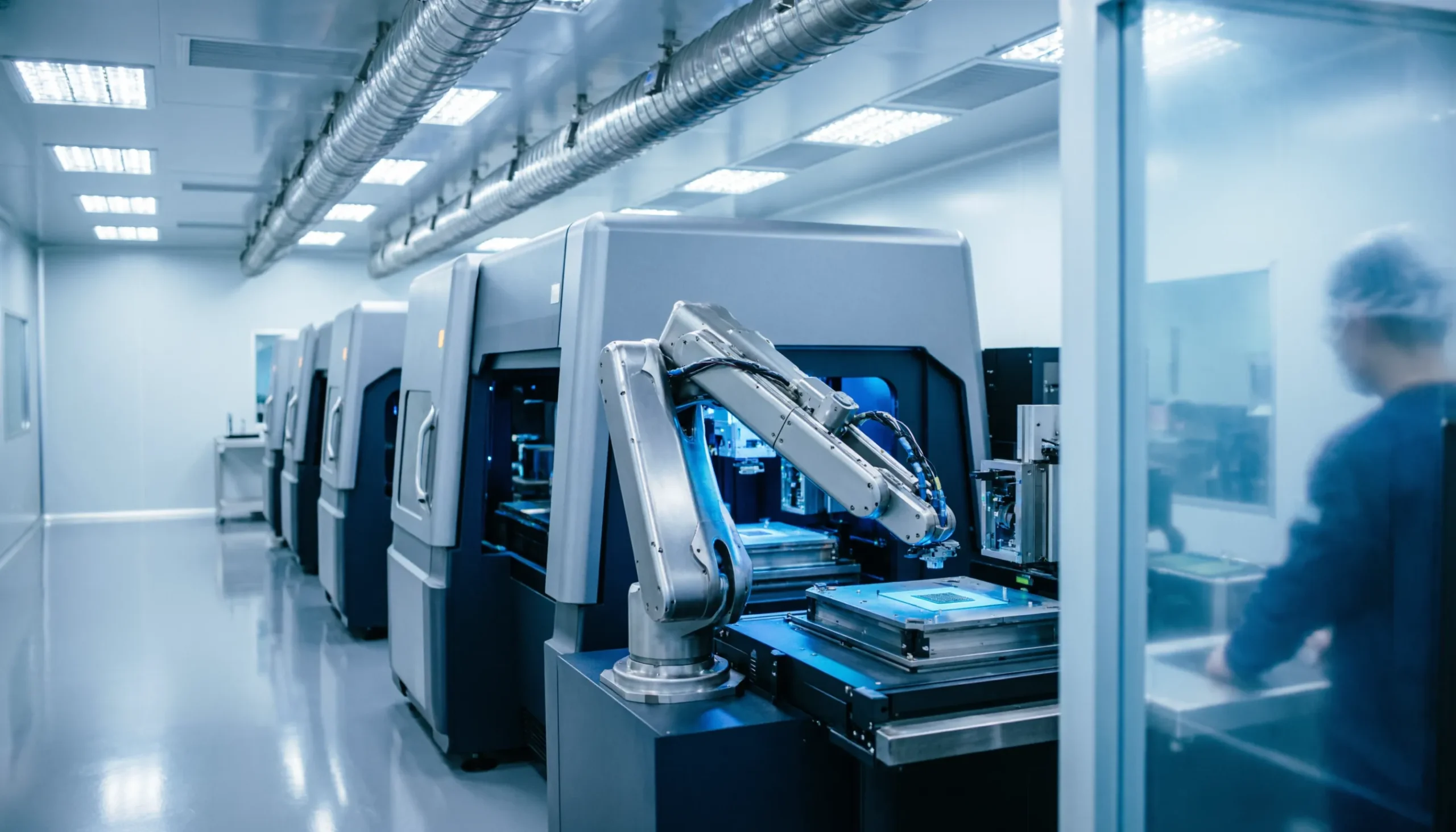
Advancing EUV Lithography Photomask Development
At the heart of this partnership lies the advancement of EUV lithography photomasks, a foundational technology for producing sub-5nm and next-generation semiconductor devices. EUV lithography enables the formation of extremely fine circuit patterns on silicon wafers by using short-wavelength light, significantly surpassing the resolution limits of conventional deep ultraviolet (DUV) lithography systems. As a result, EUV-based manufacturing supports the fabrication of transistors with smaller footprints, higher density, and improved electrical efficiency.
DNP intends to accelerate both development and mass production readiness of EUV photomasks tailored for 2nm logic processes, ensuring that Rapidus can secure a stable and high-quality mask supply as it scales toward volume manufacturing. The initiative encompasses improvements in mask blank quality, patterning precision, defect inspection technologies, and production throughput optimization. By investing early in production infrastructure and process refinement, DNP seeks to establish high-yield manufacturing systems capable of meeting stringent semiconductor industry standards while minimizing lead times for customers.
Industry Context: Rising Data Demand and Energy Challenges
The semiconductor industry is currently undergoing transformative growth driven by rapid digitalization, artificial intelligence deployment, cloud computing expansion, and the proliferation of connected devices. As global data volumes surge, energy consumption associated with computing infrastructure has become an increasingly pressing challenge. Data centers, high-performance computing systems, and AI accelerators demand chips that deliver greater computational power without proportional increases in power draw. Next-generation semiconductors manufactured using EUV lithography represent a critical solution to this dilemma. By enabling denser transistor packing and more efficient device architectures, 2nm-class semiconductors can significantly improve performance per watt metrics.
Reducing overall energy consumption while boosting processing capabilities. DNP’s investment in Rapidus reflects recognition of this broader technological shift, as well as the importance of ensuring domestic technological sovereignty in advanced semiconductor manufacturing. Through enhanced collaboration, the two companies aim to contribute to energy-efficient computing infrastructures that support sustainable digital transformation worldwide.
Government-Backed R&D and NEDO Collaboration
The partnership between DNP and Rapidus builds upon existing collaboration frameworks supported by national initiatives. In 2024, DNP was selected as a subcontractor under the Post-5G Information and Communications System Infrastructure Enhancement R&D Project led by the New Energy and Industrial Technology Development Organization (NEDO). This government-backed program focuses on strengthening Japan’s semiconductor and communications infrastructure capabilities beyond the 5G era, fostering domestic expertise in next-generation chip manufacturing technologies.
Under this initiative, DNP has been actively developing manufacturing processes tailored to 2nm-generation EUV lithography photomasks, refining techniques that ensure superior pattern fidelity and defect control at atomic-scale dimensions. The funding participation announced today further deepens this collaboration, translating R&D progress into scalable production strategies. By leveraging both public-sector support and private-sector investment, Japan’s semiconductor ecosystem gains momentum toward restoring competitiveness in the global advanced logic market.
Building a High-Yield, Short-Lead-Time Production System
A major objective of DNP’s expanded involvement is to achieve early-stage realization of high-yield and short-lead-time EUV photomask production for 2nm applications. Yield optimization is particularly critical at advanced nodes, where even microscopic defects can compromise entire wafer batches and significantly impact manufacturing economics. DNP is therefore prioritizing investments in precision inspection technologies, contamination control systems, and advanced metrology platforms capable of detecting sub-nanometer irregularities.
At the same time, reducing production lead times is essential to maintaining agility in a fast-evolving semiconductor landscape. By streamlining process flows, enhancing automation, and expanding production capacity, DNP intends to create a responsive supply framework that can support Rapidus as it moves from pilot lines to full-scale volume output. This coordinated effort strengthens the mutual partnership between the two companies and establishes a foundation for long-term technological collaboration extending beyond the 2nm generation.
Positioning EUV Photomasks as a Core Growth Driver
Within DNP’s broader corporate strategy, EUV lithography photomasks are positioned as a key growth engine for its semiconductor-related business portfolio. Historically known for its strengths in printing, materials, and precision processing, DNP has strategically diversified into high-value semiconductor components that leverage its core competencies in microfabrication and materials science. The continued miniaturization of semiconductor devices presents both technical challenges and significant market opportunities, particularly in advanced logic and high-performance computing sectors.
By proactively investing in EUV photomask capabilities, DNP reinforces its commitment to remaining at the forefront of semiconductor materials innovation. The company’s roadmap extends beyond 2nm technology, with ongoing development efforts targeting even finer geometries such as the 1.4nm generation and future nodes yet to be defined. These forward-looking initiatives demonstrate DNP’s intention to remain a long-term partner for leading-edge chip manufacturers operating at the most advanced technological frontiers.
Contributing to Japan’s Semiconductor Revival
Japan’s semiconductor industry has been actively pursuing revitalization strategies aimed at reclaiming a stronger presence in advanced logic manufacturing. Strategic alliances among domestic companies, combined with targeted government support, are central to this effort. DNP’s investment in Rapidus reflects a shared vision of establishing a robust domestic ecosystem capable of designing, fabricating, and supplying next-generation semiconductors within Japan.
By strengthening upstream capabilities such as photomask production, the partnership reduces reliance on overseas suppliers and enhances supply chain security. Furthermore, developing domestic expertise in EUV lithography processes fosters technological self-sufficiency while contributing to global semiconductor innovation. As Rapidus advances toward its 2027 mass production target, DNP’s technical and financial backing will play a crucial role in ensuring that Japan remains competitive in the rapidly evolving global semiconductor landscape.
Looking Toward 1.4nm and Beyond
While immediate efforts concentrate on enabling 2nm mass production, DNP is already setting its sights on future technology nodes, including 1.4nm and beyond. Achieving such extreme miniaturization will require breakthroughs in materials engineering, pattern transfer precision, and defect mitigation techniques.
The complexity of EUV photomask fabrication increases exponentially as feature sizes shrink, demanding continuous innovation in blank substrates, absorber materials, and inspection technologies. DNP plans to sustain proactive capital investments and collaborative R&D initiatives to address these challenges head-on. By anticipating future industry requirements and maintaining close coordination with partners like Rapidus, DNP aims to establish itself as a long-term leader in advanced photomask solutions.
Strengthening a Long-Term Strategic Partnership
The funding participation marks more than a financial transaction; it symbolizes a deepening strategic alliance between DNP and Rapidus built upon shared technological goals and mutual trust. Over the past several years, both companies have cultivated a collaborative framework encompassing R&D, process optimization, and manufacturing readiness initiatives. The latest investment strengthens this foundation and provides additional momentum as Rapidus approaches critical commercialization milestones. By aligning investment, technology development, and production scaling efforts, the two organizations are positioned to accelerate innovation cycles and enhance competitiveness on the global stage.
Through sustained investment in EUV lithography photomasks, proactive technology development for next-generation nodes, and strengthened collaboration with Rapidus, DNP reaffirms its commitment to supporting Japan’s semiconductor industry growth. As the industry navigates the transition to 2nm mass production and prepares for even finer geometries in the years ahead, the partnership stands as a strategic pillar in advancing energy-efficient, high-performance semiconductor technologies that will power the digital economy of the future.
Source Link:https://www.businesswire.com/