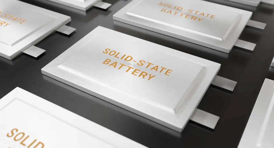
ITEN, a global leader in micro solid-state batteries, has announced a pivotal technological achievement in collaboration with the Institute of Microelectronics (IME), a research institute under Singapore’s Agency for Science, Technology and Research (A*STAR). Together, the two organizations have successfully integrated ITEN’s cutting-edge micro batteries into A*STAR IME’s advanced packaging platform, marking a breakthrough that could redefine how energy storage is embedded in next-generation electronic devices.
This accomplishment is more than a technological milestone—it signals a major shift in how power solutions can be designed for compact, high-performance electronic systems. The achievement paves the way for in-package energy storage that enables efficient, miniaturized, and highly reliable system-in-package (SiP) designs, addressing key challenges in the ever-evolving microelectronics industry.
A Breakthrough at the Intersection of Energy Storage and Advanced Packaging
The integration of solid-state micro batteries at the wafer level represents a significant leap in packaging technology. Traditionally, energy storage components such as batteries or capacitors are attached externally to electronic systems, adding bulk, complexity, and potential points of failure. By embedding ITEN’s micro solid-state batteries directly into the SiP at the wafer level, the partners have effectively eliminated these limitations.
This innovation is particularly relevant for applications where space constraints, power efficiency, and reliability are non-negotiable, such as wearables, medical implants, IoT sensors, and compact consumer electronics.
With this successful integration, the collaboration has demonstrated the feasibility of combining non-volatile energy storage with advanced semiconductor packaging techniques, streamlining the design and manufacturing process while enhancing overall device performance.
Key Advantages of Integrated Solid-State Batteries in Advanced Packaging
The breakthrough achieved by ITEN and A*STAR IME brings several tangible benefits that address critical industry demands:
1. Enhanced Energy Efficiency
By embedding micro batteries within the package, the integration minimizes energy losses typically associated with longer interconnections and external wiring. The close physical proximity of the power source to the active electronic components ensures maximum energy transfer efficiency, leading to better performance and reduced power consumption.
2. Space-Saving Compact Design
In an era where device miniaturization is paramount, embedding batteries at the wafer level significantly reduces the overall footprint of electronic systems. This enables the development of ultra-compact devices without compromising on energy storage capacity or system performance, opening up possibilities for sleeker and more versatile product designs.
3. Improved Reliability and Durability
Integrating the power source within the package reduces the need for additional connectors, solder joints, and external components—elements that often represent potential failure points. Fewer interconnects translate to higher mechanical robustness and greater long-term reliability, which is especially crucial in mission-critical applications such as medical devices and industrial IoT.
4. Simplified Assembly and Manufacturing
The wafer-level integration streamlines the manufacturing process by reducing assembly complexity. With fewer discrete components to handle, manufacturers can achieve higher production yields and lower overall costs, while also simplifying supply chain logistics.
5. Environmentally Friendly and Sustainable
ITEN’s micro batteries are designed with sustainability in mind. Free from hazardous materials like lithium in its liquid electrolyte form, they present a safer and more eco-friendly alternative. Additionally, longer device lifespans and reduced dependency on external power modules contribute to lower electronic waste, aligning with global sustainability goals.
Strategic Collaboration with Far-Reaching Industry Implications
The successful partnership between ITEN and ASTAR IME showcases the power of strategic collaboration between innovative technology companies and advanced research institutions. Both organizations bring complementary strengths to the table—ITEN with its proprietary solid-state battery technology, and ASTAR IME with its expertise in advanced packaging architectures, materials engineering, and microelectronics integration.
Their joint efforts have not only resulted in a technological breakthrough but have also laid the foundation for the next generation of SiP solutions that seamlessly integrate power sources at the chip level.
Target Applications and Market Opportunities:
- Consumer Electronics: Smartwatches, earbuds, fitness trackers, and other wearables requiring compact, long-lasting power sources.
- Medical Devices: Implantable devices and portable diagnostic tools where reliability and miniaturization are critical.
- Industrial IoT: Sensors and edge computing devices deployed in harsh environments, where durability and maintenance-free operation are essential.
- Automotive Electronics: Advanced driver-assistance systems (ADAS) and in-vehicle sensors requiring efficient energy management in limited space.
- Defense and Aerospace: Ruggedized electronic modules for mission-critical applications demanding high reliability.
Voices from the Collaboration: Executive Perspectives
The significance of this breakthrough has been underscored by leadership from both organizations.
Terence Gan, Executive Director of A*STAR IME, remarked:
“We are pleased to collaborate with ITEN to develop breakthrough advanced packaging technologies that meet the needs of the growing microelectronics market. Such efforts will enable new applications of SiP, creating new market opportunities and addressing the increasing demand for energy-efficient and compact solutions.”
On ITEN’s side, Vincent Cobee, CEO of ITEN, highlighted the critical role of A*STAR IME’s expertise:
“A*STAR IME’s strong knowledge and expertise in advanced packaging technologies support us in accelerating the development of new micro batteries optimized for integration into SiP. This is a major step forward in addressing the challenges of energy efficiency across a wide spectrum of applications.”
ASTAR IME: Driving Innovation in Advanced Packaging
The Institute of Microelectronics (IME) under A*STAR has long been at the forefront of advanced packaging research. Its comprehensive approach focuses on three core architectural families:
- High-Density Fan-Out Wafer-Level Packaging (HD FOWLP)
- 2.5D Interposer and 3D Interposer Integration
- Photonic and Heterogeneous Integration Platforms
From these core architectures, IME has developed eight specialized technology platforms that underpin its packaging innovations:
- Mold-First FOWLP
- Redistribution Layer (RDL)-First FOWLP
- Passive Interposer
- Active Interposer
- Photonic Interposer
- Wafer-to-Wafer (W2W) Hybrid Bonding
- Chip-to-Wafer (C2W) Hybrid Bonding
- Chip-to-Wafer Micro-Bump Integration
Beyond platform development, A*STAR IME also pioneers advanced manufacturing techniques, comprehensive electrical-thermal-mechanical (ETM) modeling, and package process design kits (PDK) that serve as critical tools for the microelectronics ecosystem.
Their collaborative approach with industry players, from startups to global corporations, ensures that research innovations are translated into tangible, commercialized solutions.
The Future of Integrated Energy Storage in SiP
The collaboration between ITEN and A*STAR IME is more than a singular achievement—it’s a strategic step towards the future of energy-efficient microelectronics. As the industry continues to evolve, the demand for devices that are smaller, more powerful, and more energy-efficient will only intensify.
By successfully embedding solid-state micro batteries at the wafer level, ITEN and A*STAR IME are setting the stage for the next generation of electronic systems where power is no longer an external afterthought but an intrinsic part of the package design.
This integrated approach will be pivotal for enabling autonomous IoT devices, self-powered sensors, and new wearable form factors that require ultra-compact energy solutions. Furthermore, the eco-friendly nature of solid-state batteries aligns with global initiatives for greener electronics manufacturing, contributing to broader environmental sustainability goals.
A Defining Moment for Energy Storage and Packaging Technology
The announcement from ITEN and A*STAR IME represents a defining moment in the evolution of energy storage and advanced packaging technologies. Their achievement addresses critical challenges of device miniaturization, energy efficiency, and system reliability, while also contributing to the broader objectives of sustainability and innovation.
As this technology progresses from lab-scale demonstrations to large-scale manufacturing and real-world applications, it holds the potential to transform multiple industries, from consumer electronics to healthcare and beyond.
With ongoing collaboration and continuous innovation, ITEN and A*STAR IME are poised to shape the future of System-in-Package designs with built-in energy storage, driving the microelectronics industry towards a smarter, more efficient, and sustainable future.