
OKI Launches OKI Berlin Lab R&D Center to Accelerate Photonics Innovation and Global Deployment
OKI, a leading global technology company headquartered in Tokyo (TOKYO: 6703), officially established the OKI Berlin Lab research and development center on June 1, 2025, in Berlin, Germany. This strategic move marks a significant milestone in OKI’s ongoing Technology Strategy, aimed at elevating the company’s photonics technology capabilities to a world-class level while simultaneously addressing emerging social challenges through real-world, global applications.
Strengthening Photonics Technology in a Global Hub
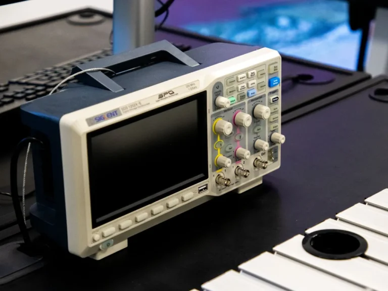
The establishment of OKI Berlin Lab underscores the company’s commitment to advancing photonics — a core technology that plays a critical role in various cutting-edge fields, including communications, healthcare, infrastructure, and manufacturing. Photonics technology involves the generation, manipulation, and detection of light, and its applications are foundational to innovations such as optical fiber sensors and compact laser vibrometers, which are pivotal for precise measurement and sensing in diverse industrial environments.
By situating its new R&D center in Berlin, OKI is positioning itself at the heart of Europe’s vibrant photonics ecosystem. Germany and the broader European Union have emerged as global leaders in photonics research and development, fostering a fertile environment for innovation through collaboration between academic institutions, government programs, and industry clusters. This dynamic landscape provides OKI with unprecedented access to cutting-edge expertise and resources, allowing for joint research projects that will accelerate enhancements in the performance and functionality of OKI’s edge devices.
Collaborative Innovation with EU Research and Industry Partners
The OKI Berlin Lab is designed as a collaborative hub that facilitates deep partnerships with leading EU research organizations, universities, and industry players engaged in photonics and optomechatronics. Optomechatronics, a specialized field that integrates optics with mechanical and electronic control systems, represents a critical frontier in advanced manufacturing technologies. OKI aims to leverage these synergies to push the boundaries of its existing technological portfolio.
This collaboration is expected to foster technological complementation, where the strengths of various partners merge to create innovative solutions that surpass what could be achieved independently. For instance, by combining OKI’s expertise in compact optical sensors with the advanced manufacturing techniques developed by European partners, new generations of edge devices can be engineered to meet the stringent demands of infrastructure monitoring, industrial automation, and healthcare diagnostics.
Moreover, the Berlin Lab will work closely with photonics clusters across the EU, regions recognized for their dense networks of specialized companies, startups, and research entities. This cluster collaboration facilitates rapid knowledge exchange, market intelligence, and accelerated technology commercialization, creating a robust ecosystem for innovation and practical application.
Global Real-World Deployment of Innovative Technologies
A key objective for the OKI Berlin Lab is to verify and validate the real-world value of the technologies developed through this joint research approach. By piloting and demonstrating these innovations within the EU, OKI will be able to refine and optimize solutions for infrastructure resilience, manufacturing efficiency, and healthcare advancement.

Once proven within European markets, these technologies are slated for global expansion, particularly targeting the Asia-Pacific (APAC) region and other international markets. This phased approach ensures that OKI’s innovations are scalable and adaptable to diverse environments and requirements, reinforcing the company’s vision of creating technologies that not only advance industry standards but also contribute meaningfully to solving social challenges on a global scale.
The Berlin Lab: A Multifaceted Innovation Facility
The new R&D center is located within a state-of-the-art incubation facility in Berlin, designed to support a range of research and business activities. It will house a team of researchers who will lead joint research projects with external partners, alongside technology marketers responsible for promoting the practical deployment of optomechatronics technologies.
An additional highlight of the center is a dedicated showroom, where OKI’s latest technological breakthroughs will be displayed. This space aims to serve as a platform for educating visitors, industry stakeholders, and potential clients on the capabilities and potential applications of OKI’s innovations, fostering a deeper understanding and facilitating engagement with the company’s evolving technology portfolio.
Aligning with OKI’s Edge Platform and Technology Strategy
The Berlin Lab launch aligns closely with OKI’s broader Technology Strategy, which was unveiled in November 2023. Central to this strategy is the “Edge Platform” concept — a solution framework designed to rapidly address societal challenges by integrating edge computing, photonics, and optomechatronics technologies.
This approach emphasizes the development of smart, connected devices capable of processing data locally (at the edge), thereby enabling real-time decision-making and reducing latency in critical applications such as industrial automation, environmental monitoring, and healthcare.
In 2024, OKI further demonstrated its commitment to open innovation by establishing a technology exploration base in Silicon Valley, USA. This initiative is focused on enhancing collaboration with startups and emerging technology companies, fostering an ecosystem that nurtures disruptive innovations. Together with the Berlin Lab’s focus on photonics in Europe, OKI is positioning itself as a global innovation leader with multiple regional hubs dedicated to technology exploration and real-world deployment.
Leadership Perspective on the Berlin Lab Initiative
Yoichi Kato, Senior Vice President, Chief Technology Officer, and Head of Technology Division at OKI, expressed enthusiasm about the new center’s potential impact:
“OKI Berlin Lab can enable OKI to strengthen core technologies through joint research with leading research organizations and photonics clusters in the EU.” He further emphasized resolve to tackle global challenges by advancing innovative technologies that will shape the future and by ensuring their deployment delivers tangible social and economic benefits.
The Future of Photonics and Optomechatronics at OKI
The OKI Berlin Lab represents not just an investment in technology, but also a strategic step toward embedding more deeply in the global innovation ecosystem. By bridging research and commercial application across continents, the company aims to maintain its competitive edge in photonics while actively contributing to solutions for pressing societal issues — from infrastructure durability and manufacturing productivity to enhanced healthcare diagnostics.
As photonics and optomechatronics continue to evolve rapidly, multi-pronged approach — combining collaborative R&D in Europe, innovation scouting in Silicon Valley, and a global deployment vision — ensures the company is well-positioned to harness emerging technologies and market opportunities.
Optomechatronics: A multidisciplinary technology that integrates optics (light-based technologies) with mechanical and electronic control systems. This field focuses on developing advanced manufacturing technologies that combine precision optics with mechanical and electronic components for innovative applications in sensing, measurement, and automation.